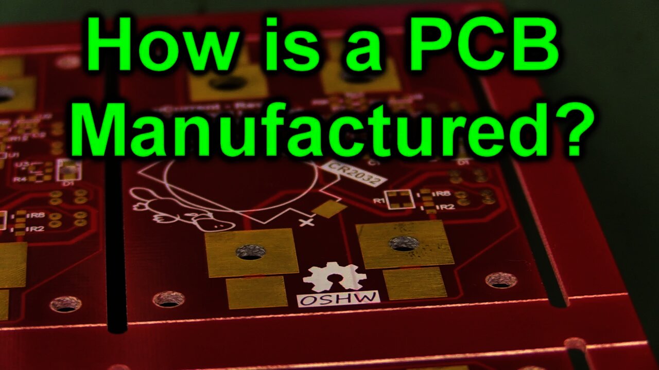
EEVblog #939 - How Is A PCB Manufactured?
How is a double sided plated through hole solder masked and silk screened component olverlay PCB manufactured?
Take a step-by-step tour of a PCB manufactuing plant.
http://www.pcbzone.net
Forum: http://www.eevblog.com/forum/blog/eevblog-939-how-is-a-pcb-manufactured/
Hard electroplated gold card edge connectors: https://www.youtube.com/watch?v=e6dH7TvqBVs
Desing for manufacture tutorial: https://www.youtube.com/watch?v=VXE_dh38HjU
DFM Automated PCB Panel Testing: https://www.youtube.com/watch?v=2zGisPMNstI&t=536s
Alba PCB Group Video: https://www.youtube.com/watch?v=P-fbIa7xlxw
Eurocircuits Video: https://www.youtube.com/watch?v=IzbmfGZDs0A
EEVblog Main Web Site: http://www.eevblog.com
The 2nd EEVblog Channel: http://www.youtube.com/EEVblog2
Support the EEVblog through Patreon!
http://www.patreon.com/eevblog
EEVblog Amazon Store (Dave gets a cut):
http://astore.amazon.com/eevblogstore-20
T-Shirts: http://teespring.com/stores/eevblog
💗 Likecoin – Coins for Likes: https://likecoin.pro/@eevblog/dil9/hcq3
-
 19:25
19:25
EEVblog Channel
1 year ago $0.05 earnedEEVblog 1585 - SCAM! Portable Kinetic Molecular Heater BUSTED
4574 -
 17:19
17:19
EEVblog Channel
6 years agoEEVblog #1158 - How To Create PCB Mod Boards
39 -
 34:27
34:27
EEVblog Channel
7 years agoEEVblog #1029 - BGA PCB Fanout
14 -
 19:09
19:09
EEVblog Channel
7 years agoEEVblog #1036 - PSU Fire PCB Repair
37 -
 1:09:58
EEVblog Channel
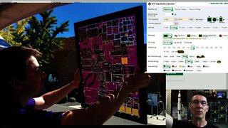
5 years agoEEVblog #1259 - PCB Manufacturing Options EXPLAINED
30 -
 38:54
38:54
EEVblog Channel
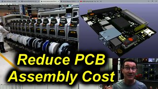
5 years agoEEVblog #1307 - TUTORIAL: PCB BOM Consolidation
25 -
 21:44
21:44
EEVblog Channel
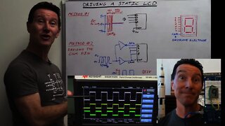
7 years agoEEVblog #1045 - How To Drive an LCD
14 -
 17:06
17:06
EEVblog Channel
6 years agoEEVblog #1142 - EEVblog LAB Tour - Before
30 -
 18:31
18:31
EEVblog Channel
6 years agoEEVblog #1123 - EEVblog Meetup 2 Electric Boogaloo
70 -
 14:58
14:58
EEVblog Channel
6 years agoEEVblog #1149 - How An Electrostatic Whiteboard Works
32