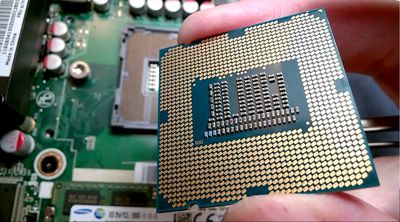
CPU processor presentation
Manufacturing is done entirely chemically
You start with sand. React it with HCL to get a liquid. Strain and vaporize it to get rid of impurities. Flow the vapor through heated graphite to get deposits of elemental silicon.
Once you get enough elemental silicon, heat it up until its a liquid. Diffuse boron gas through the mixture to make initial doping levels. Take a silicon crystal that has the right orientation and dip it into the mixture. Rotate and pull it out. As the silicon around the crystal cools, it matches the orientation of the crystal and forms a bigger crystal.
The rotations cause the cooling silicon to form into a collumn as it is pulled upwards. Eventually you end up with a REALLY BIG COLLUMN with a point on one end.
Cut your column into very thin circles called wafers. (Right now, ours are p-type because of the boron we put in earlier.) This is where the real magic begins.
The air will create a resistive coating of oxide around the semiconductor. We will now apply a series of masks on the wafer to make the chip itself.
Lets make some mosfets. Heat up the wafers to drive off moisture. Apply a thin layer of compound (photoresist) that reacts when exposed to UV light. Shoot light at it with the right pattern to create some areas where the resist is cured and some where it is not. Dump the wafer in a solution that removes the non-cured photoresist. Push hot vapors of aluminum or manganese toward the cooler wafer. They will only reach areas where the photoresist was removed. This created the n-wells for our p- mosfets.
Let the oxide grow back and deposit a layer of polysilicon to act as our gate insulator for the mosfet. Apply a mask that only covers the gates, and etch away the rest of the oxide with short wave uv light. Now push hot vapors of Boron toward the wafer to create higher concentrations of boron on both sides of the pmos gate.
Repeat the whole Boron thing we just did with aluminum to create npn gates.
Push hot nitrogen toward the wafer, apply the photoresist and etch it away to make insulating boundaries between the p/n regions and the gates.
Deposit metal on to the substrate. Apply photoresist. Etch it away to make conductive metal that goes to the different gates.
TLDR: sand -> purify -> molten SI -> doped molten SI -> giant collumn -> cut into wafer -> apply photoresist -> cure photoresist -> remove uncured photoresist -> etch photoresist -> deposit stuff ->repeat the photoresist stuff a lot
Newer cpu = more detailed photoresist = smaller mosfets = more mosfets that are better
computer desktop PC laptop tablet phone electronic
-
Exploring With Nug
3 hours agoI Found a Car Underwater… and a Bag I Wish I Hadn’t Opened!
1662 -
 LIVE
LIVE
NAG Entertainment
23 minutes agoRUMBLE ROUNDTABLE: Twitter/X Space W/ChavezFlexingtn
72 watching -
 21:54
21:54
MYLUNCHBREAK CHANNEL PAGE
19 hours agoIstanbul Should Not Exist - Pt 2
18.5K8 -
 3:44:38
Michael Franzese
1 day agoOperation Freedom Fighter: Emergency Live
64.8K37 -
 1:08:10
Jeff Ahern
3 hours ago $2.59 earnedThe Saturday Show With Jeff Ahern
17.2K7 -
 6:11:36
Grant Cardone
7 hours agoGrant Cardone LIVE: The 10X Truth That Made My First $1 Million In Real Estate
41.2K8 -
 2:28:37
putther
4 hours ago $1.84 earned⭐ Bounty Hunting on GTA⭐
20.8K1 -
 LIVE
LIVE
Total Horse Channel
1 day agoAMHA 2025 9/20
467 watching -
 1:53:15
I_Came_With_Fire_Podcast
16 hours agoThe Satanic Cults Convincing Kids to Commit Violence
52.5K24 -
![Mr & Mrs X - [DS] Created Antifa To Push An Insurgency In This Country - Ep 8](https://1a-1791.com/video/fww1/f9/s8/1/k/f/O/j/kfOjz.0kob-small-Mr-and-Mrs-X-DS-Created-Ant.jpg) 1:02:13
1:02:13
X22 Report
8 hours agoMr & Mrs X - [DS] Created Antifa To Push An Insurgency In This Country - Ep 8
160K56