The History of the Semiconductor Photomask
1 year ago
12
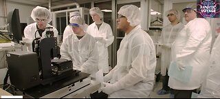
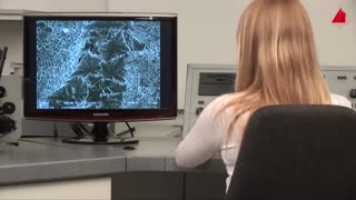
011122 Like and subscribe. This is an archive, check the link in the end if you are owner. As a fundamental part of the lithography puzzle, the photomask has a fascinating history that goes all the way back to the very beginning.
So in this video, we are going to look at this essential piece of the semiconductor manufacturing process from rubylith to EUV: The photomask.
Links:
- The Asianometry Newsletter: https://asianometry.substack.com
- Patreon: https://www.patreon.com/Asianometry
- The Podcast: https://anchor.fm/asianometry
- Twitter: https://twitter.com/asianometry
https://rumblevideoarchive.wordpress.com/
Loading comments...
-
 16:29
16:29
Asianometry Channel Archive
1 year agoSemiconductor Immersion Lithography
6 -
 15:44
15:44
Asianometry Channel Archive
1 year agoSilicon Photonics: The Next Silicon Revolution?
6 -
 0:12
0:12
KRISHUBA80
1 year agoEverything You Ever Wanted to Know About Semiconductors –
57 -
 24:27
24:27
gabfigueiro
6 months ago“The Decision of the Century”: Choosing EUV Lithography | Asianometry
30 -
 1:36
1:36
Exploring the future of technology
10 months agoThe Future of Chipmaking - Extreme Ultraviolet Lithography
-
 1:54:17
FanaticVoyage
4 months agoThe Nanotechnology Revolution-How Scientists Fabricate Nanostructures and Self-Assembled Monolayers
36 -
 17:19
17:19
Diamondarm
6 months agoSemiconductors ETF | Michael Burry NOW Bearish on Semis | ($SOXX)
111 -
 9:38
9:38
F5Tornado
2 months agoThe Scanning Electron Microscope: Material Science
110 -
 12:40
12:40
silentWrath
3 months agoCompSci; photon chip AI
18 -
 1:16:57
theabhijitchavda
2 months agoIIT Delhi Professor on Semiconductors & India's Tech Revolution | Dr Awanish Pandey on ACP
32